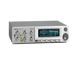
The BERTScope Clock Recovery CR Series advanced architecture measures and displays the PLL frequency response from 100 kHz to 12 MHz; the highest loop bandwidth available for jitter testing jitter testing on the market today. The first clock recovery instruments to allow full control of parameters including loop bandwidth, peaking/damping, and roll off.
Key features:
- Instrumentation quality clock recovery
- Accurate, variable loop bandwidth from 100 kHz to 12 MHz, with optional 24 MHz for the jitter transfer function (JTF) bandwidths of USB 3.0, SATA 6G, and PCIe Gen3
- Accurate, adjustable, self-measured, and displayed PLL loop bandwidth, peaking, and JTF – get the "Golden PLL" response needed for standards compliance testing
- Programmable peaking adjustment with first- and second-order roll-off capability
- USB control interface integrated into BERTScope view, or stand-alone with included BERTScope PC software
- DC-coupled data through path for accurate signal integrity
- Full and divided clock outputs with selectable divide ratios. Full-rate clock output up to 14.3 Gb/s
- Built-in equalizer function enables clock recovery under high ISI input conditions
- Data measurement capability
- Edge density measurement – determine the mark density of the signal under test
- Spread spectrum clock waveform view including dF/dt
- Ideal for spread spectrum clock (SSC) applications with large frequency excursions
- Optional direct spectral analysis of jitter components when under USB control from BERTScope or on PC using provided stand-alone software.
- Optional spectrum analyzer display with cursor measurements of jitter amplitude and frequency
- User-settable frequency-gated measurements for band-limited integrated jitter optionally available
- Preset band limits for PCI express Gen2 jitter spectrum
Specifications:
| Characteristic | CR286A |
| Input sensitivity | 100 mV single ended (typical) 50 mV differential (typical) |
| Input data rate coverage | 150 Mb/s to 28.6 Gb/s |
| Data insertion loss | 2 dB (min), 2.6 dB (typical), 3 dB (max), up to 12.5 Gb/s 1 |
| Data input voltage range | -5 V (min), +5 V (max) |
| Measured edge density accuracy | ±1%, up to 14.3 Gb/s, ±3% >14.3 Gb/s |
| Equalization range | 0 to 10 dB |
| Data output | Up to 12.5 Gb/s 1 |
Key performance specifications:
- 150 Mb/s to 28.6 Gb/s with continuous data rate coverage to include Next-generation I/Os including PCIe 3.0, 10GBASE-KR, 16xFC, 25/28 G CEI, and 100GBASE-LR-4/100GBASE-ER-4
- Full and divided clock outputs with selectable divide ratios. Full-rate clock output up to 14.3 Gb/s, half-rate clock output from 14.3 Gb/s to 17.5 and 28.6 Gb/s
- Optional PCIe 2.5, 5, and 8 gb/s PLL loop analysis (Also requires jitter analysis option)
- CR175A and CR286A offer optional higher-sensitivity data inputs with clock recovery on signals as small as 40 mV amplitude (single ended), 20 mV amplitude (differential) – no DC-coupled data through path with this option


